CEA-Leti will present new integration and packaging technologies for next-generation LiDAR optical-network driving devices in autonomous vehicles at the Electronic Components and Technology Conference, May 30-June 2, in Orlando, Fla.
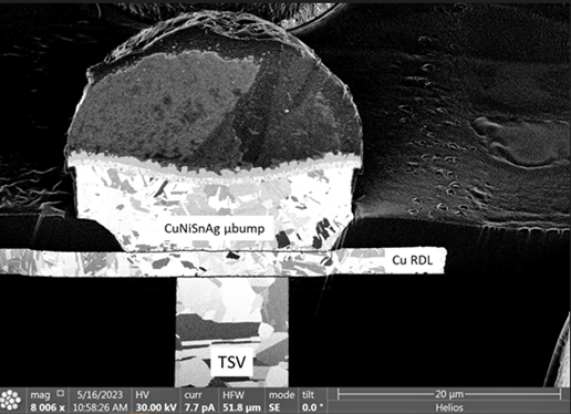
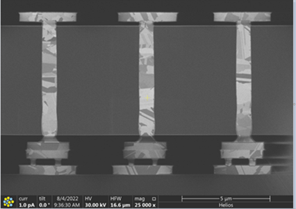
Presented in the paper, “Advanced 3D Integration TSV and Flip Chip Technologies Evaluation for the Packaging of a Mobile LiDAR 256-Channel Beam Steering Device Designed for Autonomous Driving Application", the system was developed with the institute's 3D microelectronics platform. Its 10µm-diameter mid-process through-silicon vias (TSVs) significantly improve interconnect density by distributing them on the whole backside surface of the devices. Combining 40µm fine-pitch, lead-free solder flip chip on a silicon interposer, this collective integration increases the performance and compactness of LiDARs, while lowering their cost for use in autonomous vehicles (AV). (Session 6, paper 7, Wednesday, May 31 @ 12:15 PM)
LiDAR sensors are considered to be a strong technology for ensuring safe AV driving because they can detect obstacles in the vehicle's path and calculate their distance away. First-generation LiDARs were based on a mechanically generated steering beam and were much too large to be fully integrated in a vehicle. In this research work, steering concepts were developed using wafer-level silicon technology, including optical phase arrays. A 1,550nm wavelength beam was then brought into the circuit through grating couplers, then guided through silicon-oxide waveguides to the steering area. This provides precise, latency-free information on the position and speed of obstacles surrounding road transport vehicles, independently of light conditions and with sharp angular resolutions.
Along with other CEA-Leti presentations at ECTC, the paper illustrates the institute's 3D interconnection expertise, primarily on its semiconductor wafer-level platform. System-in-package and 3D integration schemes enable mixing different technologies and/or substrate materials to address not only high-performance computing (HPC) applications requiring high-density interconnections, but also cost-sensitive applications, e.g. edge artificial intelligence and the Internet of Things (IoT).
“Our goals are to offer high-level of integration through high-density, fine-pitch interconnections to serve different requirements for a wide variety of applications,"
said Sylvie Joly, partnerships manager for 3D integration & packaging at CEA-Leti.
“Our labs' wide range of advanced technologies complement each other; for example, hybrid-bonding such as die-to-wafer and wafer-to-wafer high interconnection density is closely linked to TSVs, to keep the density for further layer or ball grid array (BGA) connections."

Additional papers:
“Demonstration of a Wafer Level Face-to-Back (F2B) Fine Pitch Cu-Cu Hybrid Bonding with High Density TSV for 3D Integration Applications"
CEA-Leti fabricated a two-layer, face-to-back test vehicle by combining fine pitch Cu-Cu hybrid bonding technology with high density TSV for applications such as CMOS image sensors and high bandwidth memories. In this work, morphological characterizations highlighted the integrity of the 3D structure. In addition, results of electrical tests on Kelvin and daisy-chain structures demonstrated high connectivity. (Session 3, paper 4, Wednesday, May 31 @ 11:15 AM)

“Process Integration of Photonic Interposer for Chiplet-Based 3D Systems"
This paper presents the process integration and technology developments of an optical network-on-chip system designed for high-performance computing (HPC). The TSV mid-process silicon photonic interposer hosts four chiplets, each integrating 16 cores, and six RX/TX drivers 3D-stacked for many-core systems. Electrical and optical characterizations of each process module are introduced and studied in the context of the system architecture. (Session 1, paper 2, Wednesday, May 31 @ 9:50 AM)
“Integration and Process Challenges of Self-Assembly Applied to Die-to-Wafer Hybrid Bonding"
CEA-Leti and Intel report the latest developments on a self-assembly technique pertaining to technology implementation in high-volume manufacturing. The self-assembly process that allows a die to be aligned through the capillary action of a water droplet placed at the bonding site showed noteworthy alignment performances with higher throughput compared to pick-and-place die bonders. The paper focuses on the integration and process challenges and reports significant improvement of bonding quality. Self-alignment capability was explored on the step height of the bonding area used for the water confinement. A 1µm-high step was reached which simplifies the subsequent processes. Finally, Cu compatibility was investigated with all the specific steps needed for the surface preparation and the impact of water on the bonding interface.
(Session 34, paper 3, Friday June 2 @ 2:40 PM)
3D Silicon Interposer for Terabit/s Transceivers Based on High-Speed TSVs"
Next-generation transceivers will be needed to manage increasing traffic growth in inter- / intra-datacenter networks. Based on silicon photonics intergrated circuits, these new transceivers will be designed to meet growing demands of complexity, bandwidth and integration. One solution involves packaging the transceivers by introducing high-speed TSVs in photonic integrated circuits (PICs). Fraunhofer IZM and CEA-Leti collaborated in the European MASSTART project to demonstrate that integration, enabling dense interconnect of high I/O count PIC packages and showing an electrical bandwidth higher than 35 GHz for these developed structures. (Session 33, paper 1, Friday June 2 @ 2:00 PM)
“Characterizations of Indium Interconnects for 3D Quantum Assemblies"
Large-scale integration of quantum technologies relies on multi-chip assemblies. In that context, CEA-Leti is focused on indium microbumps to connect chips made from different materials and technology nodes. Electrical measurements in a cryostat from 300K to 2K, as well as morphological and mechanical characterizations, were used to support this study and qualify indium interconnect technology for heterogeneous quantum assemblies. (Session 23, paper 7, Thursday June 1 @ 4:45 PM)
“Recent Progress in the Development of High-Density TSV for 3-Layer CMOS Image Sensors"
High-density through-silicon vias (HD TSVs) are combined with hybrid bonding to connect the different levels of 3D architectures that require fine-pitch interconnections. CEA-Leti has developed HD TSV of 1x10µm according to a process flow that meets the requirements of a subsequent hybrid bonding in terms of surface flatness. A median resistance of 0.7 Ω was measured on Kelvin structures and a yield of 100 percent was obtained on daisy chains made of 10,000 TSVs. The aging tests revealed no failure after 2,000 hours of high temperature storage at 150°C, or after 2,000 cycles of thermal cycling test between 55°C and +150°C. The TSVs were then qualified in a two-layer face-to-back test vehicle in anticipation of their implementation into a complete three-layer smart imager. (Session 28, paper 4, Friday June @ 11:15 AM)
CEA-Leti's Stéphane Bernabé will co-chair the special session on Photonics Packaging, May 30 at 1:30 – 3:00 p.m.
In addition, institute experts will be onsite at booth 234 and available to discuss the findings in the presentations.