As early as 2015, the Rossignol group turned to CEA-Leti to conduct R&D on the evolution of market needs. Quantified self* was already well developed in the sports world. Introducing a disruptive innovation is a complex and risky process, even for companies as experienced as Rossignol. It therefore makes sense to collaborate with an institute for technological research with the necessary skills and resources to support the company in their approach. This partnership has been beneficial for both parties: for Rossignol, by offering a richer ski experience, while it was an opportunity for CEA-Leti to improve embedded data-gathering devices using artificial intelligence.
*Developed in the United States, quantified self is a practice that brings together tools, principles, and methods that enable people to measure, analyze, and share their own personal information.
Electrical junctions are essential to the proper functioning of integrated circuits. While they happen to only make up a small proportion of the total of a device’s weight, their manufacturing process requires a great deal of energy and materials. The process therefore must be optimized to reduce their impact while ensuring state-of-the-art performance. This is specifically the challenge on which Nada and Philippe have focused their research.
Following two years in a preparatory course in Morocco, and three years at Grenoble INP Phelma studying nanotechnology, Nada Zerhouni Abdou joined CEA-Leti for an internship, before doing her thesis on the characterization of SOI substrates using an EZ-FET. This device features several advantages in terms of planetary resources, since it requires significantly fewer stages compared to a standard transistor. Her device is now ready to be integrated into a low-temperature substrate for characterization following source and drain doping and dopant activation using nanosecond laser annealing. Next stage: finding an alternative for EZ-FET substrate integration that does not require doping. Nada received the Best Young Award for her innovating scientific results given her young age.
Following a PhD in materials chemistry, Philippe Rodriguez has been working at CEA-Leti for ten years. His research findings on germanium-tin (GeSn) junctions all involve the same issue: the instability of tin makes it quite fragile when contact between the two layers is created using regular annealing process, which can cause it to segregate. To tackle this, Philippe uses a nanosecond annealing process, which creates a solid-state reaction between nickel and the GeSn component. This both reduces the thermal budget and stabilizes the junction while retaining the desired photonic properties. Philippe received the Best Paper Award for a solution that could have a significant impact for the scientific community.
Thomas Ernst received his degree in Electronics Engineering, his PhD, and accreditation for PhD supervision from the Grenoble Institut National Polytechnique (France). Following advanced SOI CMOS characterization and modelling with CNRS and STMicroelectronics, he joined CEA-Leti in 2000 to lead different research projects with industrial partners.
His team published several improvements on stacked nanosheet gate-all-around transistors (called at that time nano-beams or MBCFET® by Samsung) in 2006 and later, in collaboration with STMicroelectronics using an original so-called silicon- on-nothing technology developed by CNET, STMicroelectronics and Leti. This technology is being introduced for sub 5nm CMOS. He is now scientific director at CEA-Leti, where he oversees long-term research strategies and scientific partnerships. In 2009, he received an ERC to study multiphysics integrated nano-sensors for complex gas analysis in collaboration with Caltech. He has also been a senior member of the Institute of Electrical and Electronics Engineers (IEEE) since 2015. With a portfolio of more than 20 patents, he has authored or co-authored more than 180 articles for technical journals and international conferences.
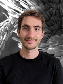
Raphaël Feougier
Congratulations to Raphaël Feougier for his award-winning paper at the 2023 SPIE Advanced Lithography event!
They are the hundreds of unit structures, ranging from 5 to 50 µm that can be seen on the surface of most insect eyes. These microlenses, which comprise an anti-reflective (AR) architecture, help a large amount of a light source converge toward photoreceptor cells, thus facilitating light trapping in dark environments. But that is not all, as these anti-reflective nanostructures also enable a surface's self-cleaning feature. For arthropods, this is a question of survival, while Raphaël sees it as a source of inspiration for improving energy efficiency in devices such as photovoltaic panels or imagers, which could greatly improve the trapping of light.
Raphaël received a DUT in Chemistry in Grenoble, before earning a professional degree on a work-study basis at the CNRS. He then continued his studies in Toulouse, where he got a Master’s in Materials Science and Engineering and Surface Treatment. Following his Master’s degree, Raphaël landed an internship at CEA-Leti, where he worked on the selective deposition of materials on substrates. He went on to earn a thesis at CEA-Leti, where he focused on the manufacturing of microlenses using grayscale lithography combined with a self-assembly process of block copolymers.Grayscale lithography (300 mm) participates in creating microstructures which, through the self-assembly of block copolymers, can then integrate anti-reflective nanostructures. These two manufacturing processes make it possible to create and control complex or hierarchical microlens structures. For now, Raphaël has found an ideal compromise between assembly height and density, as the self-assembly of PS-b-PMMA ([polystyrene-block-poly(methyl methacrylate) copolymers on a non-planar surface remains challenging. This would therefore provide energy efficiency for high-power devices. Furthermore, the process has direct access to CEA-Leti’s industrial equipment.
Raphaël is continuing to look for the best way possible to implement this technological innovation, and he already has filed a patent.
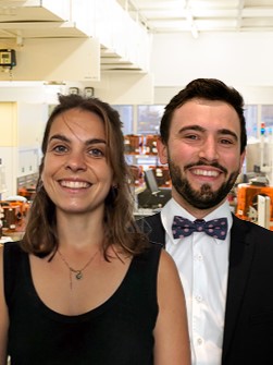
Justine Lespiaux & Marvin Frauenrath
Congratulations to Justine and Marvin for their Best Student Presentation Award at ECS 2022!
Constantly yielding important breakthroughs, epitaxy research is an extremely dynamic field. Epitaxy involves developing techniques to produce high-quality monocrystalline films with specific properties. Accurately controlling film growth, doping, and heterostructure formation has turned the method into a crucial component for the semi-conductor industry, enhancing the performance, scalability, and integration of semi-conductors.
Justine studied the epitaxial growth of IV-IV semi-conductor materials such as Silicium-Germanium (SiGe) or doped silicon. Her research involved determining the growth characteristics and incorporation of dopants, which revealed potential applications for devices and made it possible to grasp their properties in a different light. Her next goal is to integrate this process into a device as a way of improving its energy efficiency. Attending conferences remotely rather than flying, Justine takes sustainable development issues to heart both in her everyday life and in epitaxy.
Marvin rose to the challenge of co-integrating innovative materials with standardized industry equipment by using the RP-CVD (Reduced Pressure-Chemical Vapor Deposition) process. A contact resistance reduced via strong doping levels and an improved electrical confinement were used to manufacture photodiodes on Silicon Germanium Tin (SiGeSn). They demonstrated improved light-emitting intensity when integrated in photonic devices compared with photodiodes that had doped Germanium (Ge) contact layers. The wavelength range covered by the photodiodes is promising for their use as CMOS-compatible components, including to detect gases inexpensively. Having developed an optical laser device that works at room temperature, Marvin's next goal is to design a laser that will work electrically under the same conditions.
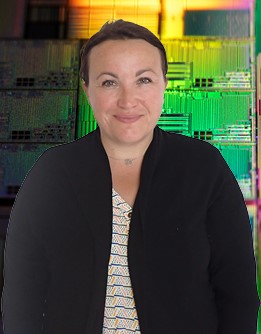
Aurélia Plihon
Congratulations to Aurélia Plihon for her "Outstanding Interactive Presentation Paper" award at ECTC 2022!
Advanced 3D packaging is a complex technology that is expected to become increasingly important in packaging a wide range of electronic devices in various fields such as IoT, AI, or medical fields. Finding viable solutions to meet the growing global demand for new integration developments has therefore become relevant.
After completing an #engineering school in materials and a 5-year experience abroad, Aurélia joined CEA-Leti intending to work on integrating innovative 3D packaging processes, in particular Fan Out Wafer-Level Packaging (FOWLP). FOWLP involves rebuilding wafers from different chips that can be placed one on top of the other, all molded from a silica-filled epoxy (EMC: Epoxy Molding Compound). Vertical interconnections, called TMI (Through Molding Interconnection), were developed to link the chips together. She was awarded for developing a simple integration of these TMIs.
Aurelia and her team achieved impressive results and reached TMIs with an unprecedented height-to-pitch ratio, with a 225 μm height, a 50 µm diameter, and a pitch of only 100 μm.
With these results, Aurélia offers a simple solution for achieving state-of-the-art high aspect ratio vertical interconnects. It will make it possible to develop more complex integrations with a high density in FOWLP applications.
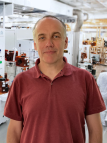
Jean-Michel Hartmann
Electronics and Photonics Division award at the 243rd electrochemical society conference, Boston, May 2023!
The surge in nanoelectronics and photonics has resulted from a need for miniaturized tools and devices that are an integral part of our lives. Additionally, it has now become necessary to consider innovation through issues involving planetary resources and energy consumption. Because it is installed in miniaturized devices, silicon-based CMOS technology is now central to these issues. This presents significant challenges for reaching a low energy consumption that aligns with current societal preoccupations.
Jean-Michel Hartmann received his PhD in Physics from Grenoble Alpes University in 1997. At the time, his research focused on solid source molecular beam epitaxy of CdTe/MnTe and CdTe/MgTe heterostructures for optical purposes. As an Imperial College postdoctoral researcher from 1997 to 1999, he studied gas source molecular beam epitaxy of Si/SiGe heterostructures for modulation-doped field-effect transistors (MODFET). Mr. Hartmann began working at CEA-Leti in 1999 as a research engineer. In 2007, he was named senior CEA expert, and Director of CEA Research in 2016.
Alongside his colleagues, Jean-Michel explored an alternative to the physical limitations of miniaturized CMOS technology by replacing Si (Silicon) by GeSn (Germanium-Tin). Thanks to the breakthrough, vertical germanium-tin transistors are strong candidates for future low-power, high-performance chips, or even quantum computers. This research led to publication in Nature magazine.
“In addition to their unprecedented electro-optical properties, a major advantage of GeSn binaries is also that they can be grown in the same epitaxy reactors as Si and SiGe alloys, enabling an all-group IV optoelectronic semiconductor platform that can be monolithically integrated on Si" the Nature paper reports.
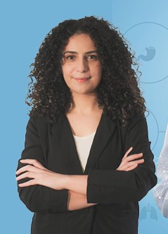
"Honorable mention" at ICASSP 2023 e-Prevention Challenge
Having begun her education in computer communication engineering at the Lebanese University of Engineering, Salam began a Master's degree in signal and image processing at Grenoble INP—Phelma. She then met CEA-Leti ambassadors, who offered her a position as a doctoral student, to work on mental health and artificial intelligence.
It's quite unique to be able to work in such a culturally rich environment, and I'm convinced that this is one of CEA-Leti's strengths.
Her interest in the workings of the human psyche led to three years researching and developing an embedded tool to understand and predict potential relapses in people who suffer from mental disorders and illnesses. Salam Hamieh only heard quite late that her supervisors had registered her for the challenge. Yet far from discouraging her, she obtained second place, with the aim of developing a tool:
A smartwatch that continuously analyzes a quantity of data that a doctor would be unable to analyze alone, and then interprets and accordingly informs the patient's specialists. The device presents a potentially viable and safe algorithm that may allow for a better understanding and prediction of relapse cases in patients suffering from bipolar disorders or schizophrenia, among other conditions.
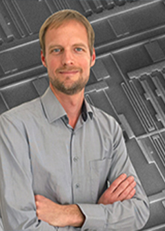
“Best Poster” award at the POWERMEMS’22 conference.
Innovation doesn’t always mean starting from scratch. It can be about reimagining existing principles to meet future needs and striking a balance between speed and energy conservation.
Gaël Pillonnet, a seasoned energy conversion expert at CEA-Leti, has come up with an ingenious solution that significantly reduces the energy consumption of traditional transistors, albeit at a slower computation speed. This opens up a host of possibilities for achieving energy efficiency and computational performance, especially in edge computing.
While microelectromechanical systems (MEMS) have been used to develop low-power computing systems before, they have been hampered by their reliance on mechanical contacts, which limit the number of logical operations possible.
Gaël Pillonnet’s approach overcomes this limitation by enabling contactless MEMS components for logic computation. By using adiabatic transformation during information processing, it is possible to achieve near-zero power consumption at lower calculation frequencies. This breakthrough in MEMS technology provides unprecedented durability to the systems in which they are integrated, making it a game changer in the field of computing.
What used to be impossible with conventional approach can now be imagined with contactless MEMS.
Next steps will therefore involve integrating this process into complex logic applications, reducing its size, and increasing the heat resistance of devices that can already withstand up to 150 °C.A.
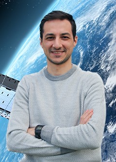
Marwan Jadid
𝗕𝗲𝘀𝘁 𝗦𝘁𝘂𝗱𝗲𝗻𝘁 𝗣𝗮𝗽𝗲𝗿 "𝗵𝗼𝗻𝗼𝗿𝗮𝗯𝗹𝗲 𝗺𝗲𝗻𝘁𝗶𝗼𝗻" 𝗮𝘁 𝗜𝗦𝗔𝗣'𝟮𝟮
The field of satellite technology is undergoing a revolution with the development of “New Space” and miniaturized antennas. As space becomes increasingly crowded and raises the need for optimized power directions, the ability to reduce the size and weight of satellite antennas while maintaining their performance is essential. Marwan Jadid delivered encouraging results in a crystal-clear presentation, showing how these advancements are expanding possibilities for applications and services that were once thought impossible.
After attending a Telecommunications engineering school and completing a RF/Microwaves Master’s degree, Marwan wanted to explore disruptive solutions involving microsatellite antennas bandwidth and efficiency and embarked on a PhD at CEA-Leti, in close collaboration with CNES. Thanks to anechoic chambers at CEA-Leti and CNES, Marwan was able to test several prototypes and find an optimal configuration in controlled conditions.
Co𝗻𝗰𝗿𝗲𝘁𝗲 𝗿𝗲𝘀𝘂𝗹𝘁𝘀
To develop innovative RF solutions, Marwan had to consider power-coupling methods, a critical aspect. He also focused on finding the appropriate design for the feed/excitation type and control near field coupled power. Marwan was pleased by fantastic performances involving a non-conventional antenna size, which will contribute to reducing EM pollution and space crowding.
By combining my understanding of field and circuit theories from my background in RF engineering, I came up with a successful design for a new solution. I am confident that my skills and experience will help me push the boundaries of what is possible in the field of Radio-frequency Engineering.”
What’s Next
As Marwan is passionate about all things applied electromagnetics, he is eager to tackle new challenges and to explore uncharted territories at CEA-Leti labs.
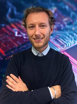
𝗕𝗲𝘀𝘁 𝗣𝗼𝘀𝘁𝗲𝗿 𝗣𝗿𝗲𝘀𝗲𝗻𝘁𝗮𝘁𝗶𝗼𝗻 𝗮𝘁 𝗘\𝗣𝗖𝗢𝗦 𝟮𝟬𝟮𝟮 𝗶𝗻 𝗢𝘅𝗳𝗼𝗿𝗱
The impetus for CEA-Leti innovations always begins with academic and industrial needs. Anthony Albanese's research on amorphous chalcogenide materials for highly nonlinear on-chip components confirm CEA-Leti's expertise at the forefront of More than Moore solutions.
After earning a scholarship to study in Grenoble, Anthony went on
to pursue a PhD at CEA-Leti, in collaboration with the Institut Carnot de Bourgogne. His aim was to explore energy efficiency issues through the inclusion of innovative materials in photonic systems while ensuring CMOS compatibility, which is essential to industrial transfer.
The chalcogenide materials he studied have promising optical properties and feature exceptional nonlinearity while retaining great transparency and good thermal stability. Special thanks go to Jean-Baptiste Dory, the former PhD student who launched the topic at CEA-Leti in 2016 under the supervision of Pierre Noé, at the Department of Advanced Material Deposition, and with Pierre's close collaborators from the University of Bourgogne in Dijon (Benoit Cluzel), FNRS at the University of Liège (Jean-Yves Raty) and at the ESRF of Grenoble with the Italian CRG beamline LISA (Francesco d'Acapito). This research make it possible to improve performance in the following areas: quantum computing, infrared sensors, telecommunications, and so much more.
Anthony had the opportunity to keep discussions going on new issues surrounding amorphous chalcogenide materials for highly nonlinear on-chip components and phase-change materials for on-chip active components and neuromorphic computing applications in the course of two oral presentations at the MRS 2022 Fall Meeting, in Boston, where he was selected for the Third Place in the judging of student presentations in Symposium
EQ04: Emerging Chalcogenide Electronic Materials – Theory to Applications. He was also able to share his knowledge and passion for materials engineering and solid-state physics through classes he gave to Master's students at INP Phelma, an experience he found extremely gratifying.
CEA-Leti has the best to offer. As a doctoral student, you are given total autonomy with a wide range of cutting edge technological tools and can collaborate with world-renowned researchers. It’s quite unique.
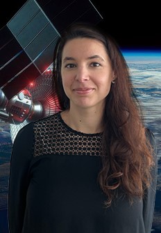
Ségolène Dinand
Space is not a very hospitable environment... especially for image sensors on orbiting satellites. Space missions are exposed to radiations from solar winds and cosmic rays. Ségolène Dinand devoted her PhD to better understanding how the radiation environment in space affects HgCdTe infrared detectors.
Over the course of her engineering studies, multiple internships in the space sector confirmed her interest in these issues. Ségolène went on to work with the European Space Agency for a year and a half, before joining CEA-Leti for her PhD, in partnership with the ISAE-Supaéro engineering institute and Airbus Defence and Space. Her PhD project was aligned not only with her scientific aspirations but also with her desire to root her research in practical applications.
In a first for her laboratory, Ségolène developed a characterization system to precisely analyze the effects of radiation on HgCdTe photodiodes. With access to the necessary equipment to cool her detectors to 90 K (-183°C), she was able to conduct experiments in conditions closely resembling those experienced by detectors in orbit. Her findings were presented at international conferences.
Her research will make it possible, firstly, to anticipate declining performance of HgCdTe detectors, and secondly, to identify parameters for increasing their resistance to ionizing and non-ionizing radiation. Orbiting infrared instruments play an essential role in greenhouse gas emissions monitoring, meteorology, astronomy and Earth observation.
Ségolène notes:
"𝑫𝒖𝒓𝒊𝒏𝒈 𝒎𝒚 𝑷𝒉𝑫, 𝒓𝒆𝒈𝒖𝒍𝒂𝒓 𝒅𝒊𝒂𝒍𝒐𝒈 𝒂𝒏𝒅 𝒄𝒐𝒍𝒍𝒂𝒃𝒐𝒓𝒂𝒕𝒊𝒐𝒏 𝒘𝒊𝒕𝒉 𝒑𝒆𝒐𝒑𝒍𝒆 𝒇𝒓𝒐𝒎 𝒎𝒖𝒍𝒕𝒊𝒑𝒍𝒆 𝒐𝒓𝒈𝒂𝒏𝒊𝒛𝒂𝒕𝒊𝒐𝒏𝒔 𝒑𝒓𝒐𝒗𝒆𝒅 𝒊𝒏𝒗𝒂𝒍𝒖𝒂𝒃𝒍𝒆, 𝒂𝒍𝒍𝒐𝒘𝒊𝒏𝒈 𝒎𝒆 𝒕𝒐 𝒕𝒂𝒌𝒆 𝒎𝒚 𝒓𝒆𝒔𝒆𝒂𝒓𝒄𝒉 𝒇𝒖𝒓𝒕𝒉𝒆𝒓 𝒃𝒚 𝒔𝒕𝒖𝒅𝒚𝒊𝒏𝒈 𝒂 𝒈𝒊𝒗𝒆𝒏 𝒑𝒉𝒆𝒏𝒐𝒎𝒆𝒏𝒐𝒏 𝒇𝒓𝒐𝒎 𝒅𝒊𝒇𝒇𝒆𝒓𝒆𝒏𝒕 𝒑𝒆𝒓𝒔𝒑𝒆𝒄𝒕𝒊𝒗𝒆𝒔."
|

Ludwig Rotsen
Best poster for his
FDN 2022 DNA Nanotech breakthrough
Ludwig Rotsen wanted to draw inspiration from life to create advanced nanotechnologies, and he has done an excellent job addressing his goal, confirming CEA-Leti’s focus on always reinventing innovation based on available resources and on demand.
After completing of the first part of his thesis in Montpellier, France, Ludwig Rotsen joined CEA-Leti to work on DNA origami for use in lithography, in collaboration with the CNRS.
The versatility and addressability of DNA are unprecedented, making it possible to broaden our catalog of 2D networks and to envision increasingly specific uses that will require nanostructures. This high addressability and the limited quantity of lithographic material mean that it is possible to generate countless structures in a relatively short timeframe (in the order of several weeks).
Thanks to the new process for depositing DNA nanostructures on silicon dioxide, Ludwig controls every 2D network interaction, and his work will enable great strides in the field of quantum computers.
Ludwig notes “𝑺𝒊𝒏𝒄𝒆 𝑰 𝒂𝒎 𝒘𝒐𝒓𝒌𝒊𝒏𝒈 𝒐𝒏 𝒂 𝒎𝒖𝒍𝒕𝒊𝒅𝒊𝒔𝒄𝒊𝒑𝒍𝒊𝒏𝒂𝒓𝒚 𝒔𝒖𝒃𝒋𝒆𝒄𝒕, 𝑰 𝒘𝒆𝒂𝒓 𝒕𝒘𝒐 𝒉𝒂𝒕𝒔—𝒕𝒉𝒂𝒕 𝒐𝒇 𝒂 𝒑𝒉𝒚𝒔𝒊𝒄𝒊𝒔𝒕 𝒂𝒏𝒅 𝒕𝒉𝒂𝒕 𝒐𝒇 𝒂 𝒄𝒉𝒆𝒎𝒊𝒔𝒕. 𝑰 𝒄𝒂𝒏’𝒕 𝒂𝒍𝒘𝒂𝒚𝒔 𝒈𝒊𝒗𝒆 𝒂𝒅𝒗𝒊𝒄𝒆 𝒐𝒏 𝒗𝒆𝒓𝒚 𝒔𝒑𝒆𝒄𝒊𝒂𝒍𝒊𝒛𝒆𝒅 𝒕𝒐𝒑𝒊𝒄𝒔 𝒊𝒏 𝒆𝒊𝒕𝒉𝒆𝒓 𝒐𝒇 𝒕𝒉𝒐𝒔𝒆 𝒇𝒊𝒆𝒍𝒅𝒔, 𝒃𝒖𝒕 𝑰 𝒂𝒍𝒘𝒂𝒚𝒔 𝒉𝒂𝒗𝒆 𝒂𝒏 𝒐𝒑𝒑𝒐𝒓𝒕𝒖𝒏𝒊𝒕𝒚 𝒕𝒐 𝒍𝒆𝒂𝒓𝒏 𝒔𝒐𝒎𝒆𝒕𝒉𝒊𝒏𝒈 𝒏𝒆𝒘!”
Both his greatest challenge and what he has most enjoyed has been participating in a project for two organizations that have different approaches. Working at CEA-Leti has taught him to better understand real-work applications for his thesis, along with issues around the transfer of his innovation to the industry market.
To close, his experience reminds us that sometimes, reorganizing what exists is a way of finding innovative solutions for tomorrow’s technologies.

Adrien Morel
Best Thesis award from the EEA Club 2022
How can we optimize energy harvesting in closed, confined environments? Adrien Morel's work on power management for piezoelectric harvesters is proof that CEA-Leti is leading the race to meet the increasing demand for energy autonomy in embedded systems in inaccessible environments.
After his first internship in our labs, focusing on piezoelectric materials, Adrien decided to extend his work during his thesis. His thesis studies involved electrically tuning the resonant frequency of a piezoelectric vibration energy harvester in order to monitor its dynamics in real time. After comparing different combinations of power harvesting strategies, Adrien implemented the most effective one in a dedicated integrated circuit.
The bandwidth of the harvester has been increased by up to six times compared to the traditional approaches in the literature.
Adrien is paving the way for more autonomous, energy-efficient systems in closed, confined environments. He has also pointed out that applications are diverse, and not always where we expect them to be! For example, this breakthrough could improve the living conditions of patients wearing medical devices in need of a constant energy supply, as it will enable energy-efficient autonomy without the need for further invasive intervention. No need to replace batteries!
"One of the Leti's biggest strenghts is that as researchers, we get the opportunity to work on interdisciplinary domains, which means we get to exchange ideas with so many people. It is rewarding, and I think it is unusual to benefit from this kind of working dynamic", he says.
But it was also a challenge for him to collaborate with so many people and to gather enough information to complete his thesis successfully! This was actually the main reason he won this prize.
Simon Deleonibus
IEEE Cledo Brunetti Award 2022
Simon Deleonibus received the IEEE Cledo Brunetti Award 2022 for more than 35 years of contribution and leadership in nanoscale CMOS device and process technologies at Thomson Semiconductor (now STMicroelectronics) and CEA-Leti!
As a chief scientist, Simon Deleonibus has inspired young CEA-Leti researchers!
About Simon’s major contributions: - 1984: Plugs principle patent for microelectronics interconnections and demonstration, now used by the entire semiconductor industry
- 1987-95: world recognized expertise on ultimate field isolation for non-volatile memories - 16Mbit-1Gbit generations - with high aspect ratios and advanced logic CMOS
- 1996: Patent for self-aligned damascene metal gate and demonstration, now used in advanced high-speed processors
- 1999: world's smallest 20nm transistor
- 1999-2016: 2D & 3D device architectures integration and Silicon Components and Technologies scientific leadership
| |
|
|
| |