
March April 2024 issue of Chip Scale Review
Because of increasing costs of advanced nodes and the difficulties of shrinking analog and circuit input-output signals (IOs), alternatives to single-die architectures are becoming mainstream. Chiplet-based systems using 3D technologies are compatible with scalable modular architectures, and with technology partitioning based on reusable intellectual property (IP) blocks. Moreover, 3D interconnects increase chip-to-chip bandwidth and limit overal power consumption. Industries across the whole range from automotive to high-performance computing (HPC) will soon be relying on advanced packaging to deliver simpler, faster, and cheaper chip designs that integrate more functions while offering greater performance and versatility. The chiplet-on-inter poser concept involves integrating a multiplicity of chips on the same silicon platform; it contrasts with large monolithic systems-on-chip (SoCs) platforms.
The active interposer extends this concept by adding smart functions at the inter poser level, such as complementary metal-oxide semiconductor (CMOS) components. The interposer, thereby, becomes more than a simple interconnection platform; it provides the foundation for analog and low-power digital and photonic functions and increased 3D communication, especially with network-on-chip architectures. In 2019, CEA-Leti and CEA-List presented the first CMOS active interposer measured on silicon, integrating power management and distributed interconnects to create an innovative scalable cache-coherent memory hierarchy. In this demonstration, six 28nm FD-SOI chiplets were 3D-stacked onto an active interposer in a 65nm process, to create a total of 96 cores [1].
To reduce the die-to-wafer (DTW) interconnect pitch, leading microelectronics manufacturers consider that direct hybrid bonding (HB), using mixed copper/oxide interfaces, will be essential for the success of future memory stacks, high-performance computing (HPC), and to support the continued application of Moore's Law. Heterogeneous 3D integration has been identified as a way to increase functionality per unit area by optimizing space in the x, y and z directions.
For over 10 years, CEA-Leti has been part of the French public Nanoelec Technological Research Institute ecosystem, gathering 22 partners from academic research institutions and industry [2]. Within this framework, to offer advanced packaging and HB solutions, we have teamed up with equipment manufacturers (SET, EVG, etc.) and adapted specific bonding processes from pick-and-place technology to self-assembly (SA) to improve yield and alignment accuracy. Today, we can bond chips from 1mm² × 1mm² to 10mm² × 10mm² by HB with interconnect pitches from 10μm to less than 5μm [3]. In addition, die spacing can be as low as 40μm. Current developments are focused on multi-stack DTW processes. We have demonstrated that signals and power supply from top-die circuits can be communicated to a substrate using through-silicon vias (TSVs) [4]. CEA-Leti is We are also working on new integration technologies such as SA. The advances made provide higher alignment performance (+/-200nm) and increased throughput (thousands of dies/h). Another key area of research relates to optimization of the temperature of the HB process, with the aim of preserving memory or active device performance.
To further improve data transmission during communication, we are contributing to the development of a disruptive approach to HPC: optical network-on-chip (ONoC) technology. Photons (light) have the potential to deliver fast on-chip communication for HPC, with increased bandwidth and reduced power consumption [5]. The main technological challenges faced by our architectural vision of an ONoC approach to chiplets were: 1) a scalable, low-profile interface between the chiplets and network; 2) decentralized routing to reduce data movement within the system; 3) thermal management compatible with optical communications; and 4) maintaining individual chiplet performance in multiple-chiplet integrations. By tackling the issues noted above, we successfully co-integrated 3D interconnections and photonic devices using a newly demonstrated approach to form 10µm diameter by 100µm high TSVs through copper metallization inside a photonic chip [6]. Thermal insulation was improved by etching 40µm diameter backside cavities beneath the optical micro-rings, leading to a 70% reduction in the power required to tune the micro-rings. Moreover, we have shown efficient thermomechanical stress management of the thinned 100µm photonic interposer for assembly processes [7].
3D sequential integration makes it possible to achieve the best possible 3D contact densities between stacked tiers (<100nm pitch). This integration is attracting strong interest for more-than-Moore applications, such as CMOS image sensors with smart, scaled pixels, or mixed-signal applications where low-voltage analog and digital devices occupy separate levels, thereby allowing their independent optimization. The introduction of intermediate back end of line (iBEOL) between the stacked transistors will add to the variety of applications that this technology can address.
TSV: a key enabling technology for heterogeneous systems
In the framework of advanced dense interconnection, we have developed TSV processes since 2006, and consequently, we have the requisite experience to contribute to the design of new modules or system architectures. We started with the TSV-last process for CMOS image sensor applications that are still being optimized for new computed tomography X-ray scanners or detectors for advanced particle physics needs. We then worked on TSV mid-process for memory on logic, and afterwards on silicon interposers application to more recent high-density (HD) TSV for logic blocks interconnections combined with hybrid density, for example. Each of the TSV developments noted above followed the same rigorous protocol, involving optimization of its electrical properties (resistance, leakage, capacitance) and qualification of reliability norms at first using passive test vehicle integration, and then moving to active wafers (sensors, power or computing technologies). In 2023, we presented results on the TSV process with an aspect ratio of 10:1, i.e., with a diameter/space of 1μm/1μm (pitch 2μm) associated with a depth of 10μm; this application was for HD copper TSVs for use in advanced imaging applications or further backside power-delivery network architectures for nano TSVs.
A test vehicle consisting of a single metal level on each side of a thinned silicon (Si) substrate bonded to a thick carrier was produced to develop and optimize the process flow, ensuring that it would be compatible with the constraints of the subsequent HB process. Electrical resistance measurements revealed a median value of 0.7Ω on Kelvin patterns, with a 100% yield achieved on 10,000-TSV daisy chains. Remarkably, no failures were recorded during extensive reliability testing, including 2,000 hours of high-temperature superconducting (HTS) at 150°C, and 2,000 thermal cycling test (TCT) cycles between -55°C and +150°C [8]. These results, shown in Figure 1, , are a major milestone for very highly-integrated architectures based on multiple-layer wafer-to-wafer integrations. Emerging data will be the subject of a forthcoming conference presenting even more integrated TSVs landing on aggressively thinned metal 1, to mimic the integration of 22nm or smaller nodes.
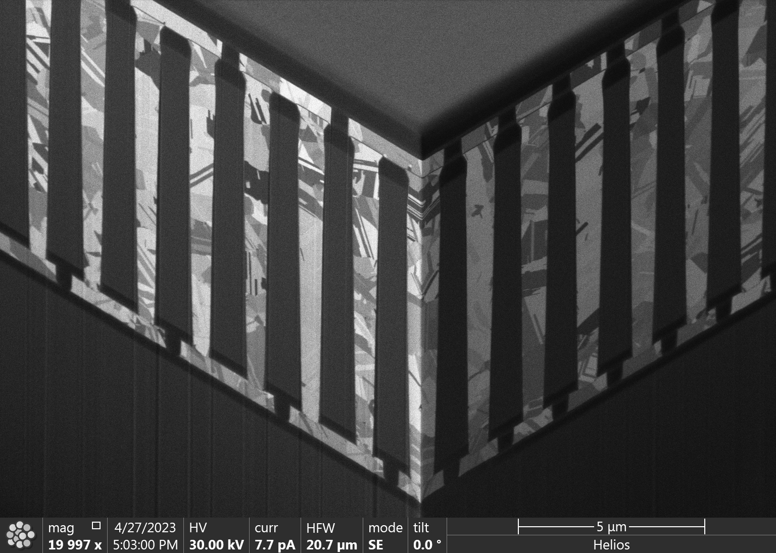
Figure 1: Field higher beam cross section of a HD TSV (Ø=1μm H=10μm) daisy chain.
SOURCE: CEA-Leti/R.
Active interposers: enhancing photonic and HPC applications
From an architectural point of view, our interest in interposers started in 2010 with the development of large passive interposers [9]. Since then, this theme has followed its own roadmap alongside developments in advanced HPC, requiring increased bandwidth, reduced latency and greater power efficiency. From passive interposers, the technology has moved to active interposers including active 3D links and embedded DC-DC (direct current) convertors for pinpoint power delivery. It has finally matured for use in photonic interposers, making it possible to overcome the latency wall that emerges with increasing chip-to-chip distances even with these on-chip architectures. For each of these approaches, dedicated technological developments were required, starting from passive interposers with integration of the first 10µm diameter by 100µm high TSV [10]. The absence of devices on the substrate meant that less emphasis was required on thermal oxidation and planarization or metallic contamination of active parts, which facilitated TSV integration.
Moving to an active interposer, the compatibility with the production fab for BEOL completion represented a real challenge in terms of copper protrusion from TSVs, or other defects. These have been tackled thanks to the increased maturity of the TSV filling and annealing processes, combined with systematic close inspection of each TSV in the closed loop by industrial process teams to determine optimal process points. These developments related to photonic interposers represent a real breakthrough in terms of interconnections, as mentioned, and demonstrate the convergence of the photonic and 3D integration roadmaps. The TSV aspect ratio and the metallization process have remained almost unchanged since the first integration, but the inclusion of a 2µm thick buried oxide (BOX) to avoid parasitic coupling between waveguides and the underlying silicon was a real challenge. First, the TSV etching was fully redeveloped to produce smooth sidewalls for later metallization and to eliminate the silicon etching below the BOX; then, the thermomechanical deformation of the thin substrate due to the thick BOX had to be compensated by balancing all the between-layer stresses linked to frontside and backside interposer integration.
Figure 2: Photonic waveguides and micro bumps on a Popstar Interposer.
SOURCE: CEA-Leti/J. Charbonnier
These adjustments were mandatory for the assembly of the top dies of the Popstar photonic interposer demonstrator (Figure 2) hosting four computation chiplets and six electro-optical driver chips. The successful TSV integration in this photonic interposer was demonstrated by assessing the electrical yields and electro-optical performances of TSV chains [11]. The first functional intermediate demonstrators have just been assembled (Figure 3). This study contributes to the ongoing progress in computing systems, particularly in the realm of HPC, by providing insights and solutions to integrate optical communication technologies within a heterogeneous computing architecture.
Figure 3: STARAC frontside module: Popstar photonic interposer, 4 chiplets and
6 electro-optical drivers in 28nm FD-SOI. SOURCE: CEA-Leti/R. Franiatte
By combining 3D integration with mid-process TSV and advanced packaging, based on small-pitch flip chips and optic fiber pigtailing, heterogeneous integration of a photonic device on a silicon interposer was achieved. This represents the functional demonstration of the next generation of beam steering for a light detection and ranging (LiDAR) designed for autonomous vehicle driving. Figure 4 shows integration of the flip chip in an optical phase array (OPA) generating the laser beam scanning a silicon interposer, thanks to a 10µm TSV and 40µm pitch copper pillar. The 256 channels of the OPA are wire bonded to a printed circuit board (PCB) and an 8-channel fiber array is connected to deliver the laser beam. The system is fully functional and complies with advanced driver assistance systems (ADAS) specifications for beam scanning angles, divergence and power consumption [12].

Figure 4: Solid-state optical phase array photonic device for an autonomous
vehicle driving light detection and ranging (LiDAR) packaged device using a midprocess
TSV and a fine-pitch flip-chip process on a silicon interposer.
SOURCE: CEA-Leti/ N. Miloud-Ali
Hybrid bonding: a solution for heterogeneity
Hybrid bonding is a maturing technology in advanced fabs that is essential to the emergence of 3D devices. This technology is similar to direct bonding, but is applied to mixed Cu/dielectric surfaces to create an electrical interconnection between two parts. Direct bonding is quite distinct from thermocompression and adhesive bonding, which require temperature and pressure, or additional materials such as polymer, respectively, to ensure contact between the two surfaces. Following stringent surface preparation i.e., topography and cleanliness direct bonding is spontaneous, requiring no external loading.
Figure 5: Die-to-wafer hydrid bonding. SOURCE: CEA-Leti/L. Sanchez
HB is particularly suitable for interconnection densities with pitches from 1µm to 10µm. The race to achieve higher interconnection densities is the main driver on the HB development roadmap for HPC or imaging applications [13]. However, HB is also more reliable and results in a thinner total stack compared to micro-bumps, which are used in automotive applications and high-bandwidth memory applications.
HB has matured enough to have entered mass production, especially for stacked image sensors in its wafer-to-wafer version. Devices with two-die stacks are available on the market, and advanced research on three-die stacks are advancing well. Die-to-wafer (DTW) hybrid bonding will dramatically enhance designer creativity as several advanced technology nodes and substrates can be assembled on a single interposer to produce heterogeneous 3D (Figure 5).
For future research on HB, the development of low-temperature processes will be key to addressing technologies with a low thermal budget. For example, SA is being explored, as are horizontal die-to-die interconnections by HB [14]. In the latter context, interposer or bridges should make it possible to overcome stepper limitations.
3D sequential integration: optimizing 3D contact densities
The strategy adopted at CEA-Leti to introduce iBEOL between sequentially stacked tiers introduced the following new challenges: 1) a limitation of the top CMOS field-effect transistor (FET) thermal budget process to 500°C, and 2) the need to ensure a safe return to only front end of line (FEOL) contamination when processing the top transistor. Figure 6 shows the recent demonstration of one such integration [15]. Above a standard industrial 28nm fully-depleted silicon-on-insulator (FD-SOI) platform including four Cu/ultra low-k (ULK) dielectric metal levels, the top CMOS device layer was fabricated
within a 500°C thermal budget. A new Bevel Wrap Contamination module was introduced to allow a safe return in a front end of line FEOL contamination before proceeding with direct bonding of the top channel and full device processing in a FEOL clean room with state of the art 300mm tools. The CMOS FD-SOI top devices produced showed performance levels similar to those of high-temperature FD-SOI devices. The demonstrations of a ring oscillator and a high dynamic range (HDR) pixel, which are firsts, take 3D sequential integration to the next level in terms of maturity.
CEA-Leti We envisions 3D sequential integration in the fields of scaled and smart imagers, radio-frequency (RF) applications and highly efficient computing. The toolbox developed includes low-temperature devices with digital (<1V) and analog units of merit (>2.5V) fabricated at low temperatures on monocrystalline channels, with the goal of achieving fabrication of top-quality devices at low temperatures without limiting performance compared to traditional high-temperature CMOS devices. This capacity would be useful across a wide range of applications.
Figure 6: Transmission electron microscopy (TEM) cross section of the 2-CMOS layer stacking including
iBEOL with Cu/ULK 28nm. SOURCE: CEA-Leti
Advanced packaging: toward a European 3D strategy
Future HPC, artificial intelligence (AI), image sensors, smart displays, etc., will be based on advanced packaging and 3D integration of components in increasingly complex architectures. The United States is at the forefront of this trend thanks to concrete examples from NVIDIA, AMD, and Intel. Strong competition also exists in Asia between giant players like TSMC and Samsung. Europe must reduce the gap with the U.S. and Asia, who are investing heavily in this advanced packaging and 3D. Indeed, performance improvements in the latest semiconductor nodes will not be sufficient to deal with the needs of emerging applications (e.g., generative AI). Advanced packaging is an alternative path allowing chips fabricated using different technologies to be combined to optimize performance and cost of the final “chip” assembly.
Summary
CEA-Leti is pursuing its historical interests in heterogeneous integration and 3D, and developing an ambitious roadmap for system and technology co-optimization. To support European ambitions for the semiconductor industry, we have also established partnerships with other European research and technology organizations (RTOs), like IMEC imec, Fraunhofer Institute, and Tyndall. As part of this, CEA-Leti has joined PREVAIL, the multi-hub Test and Experimentation Facility for edge AI hardware [16]. In addition to technological developments, CEA-Leti we are also addressing environmental challenges through life-cycle assessments of technologies, low-power systems enabled by 3D, exploration of chip re-use, etc.
Acknowledgment
This work was partly supported by the French National program “IRT Nanoelec, n° ANR-10-AIRT-05 and by European Union’s H2020 under the grant agreement n 958472 (Tinker) and n 780548 (3D-MUSE). This work is part of the IPCEI Microelectronics and Connectivity and was supported by the French Public Authorities within the frame of France 2030.
About Jean-Charles Souriau
Jean-Charles Souriau is a scientist leader in the field of wafer-level packaging for more than 20 years at CEALeti,
Grenoble, France. He has worked at the Electronics and Information Technology Laboratory, French
Atomic Energy Commission, Micro and Nanotechnologies Campus. He is chair of the French chapter of the
IEEE Electronics Packaging Society and Technical Director of IMAPS France. He received the PhD degree in
physics from the U. of Grenoble, France in 1993.