Five advantages of silicon spin
Published on 8 February 2024
Body text 2
The silicon approach, which leverages well-established CMOS technologies, still faces significant developmental challenges, but it offers a number of fundamental advantages that make it appealing as a way forward. Some of the most important of these are:1-
- Device operability at temperatures in the ~1K range, rather than the mK range (near absolute zero) required for superconducting approaches. While this may not seem like a large difference, the difficulty of achieving and maintaining lower temperatures increases exponentially as they approach absolute zero. This extra margin in thermal budget allows for the operationof larger systems with more embedded classical control electronics.
- Improved resistance to decoherence, due to the characteristics of silicon. The phenomenon of decoherence is a fundamental challenge to quantum computing, and one major source in semiconductor spin qubits is the interaction between the magnetic moments of electron and nuclei spins. While III-V semiconductor materials, as used in some photonic-oriented quantum development efforts, have non-zero total nuclear spins, the majority isotope of Si, 28Si (which represents 95% of natural Si), has no net nuclear spin. Additionally, natural Si may be isotopically purified almost as far as needed (the state-of-the-art is above 99.99%) using centrifugation. It results in a remarkably clean magnetic environment for the qubits and therefore longer electron spin lifetimes.
- Speed of operation. Thanks to a gate-defined structure that all ows tight coupling, speed is in the μs range for all types of operations. This ensures reasonable calculation times, on the order of billions of operations per hour, which is well in line with the current state of the art in quantum processing.
| 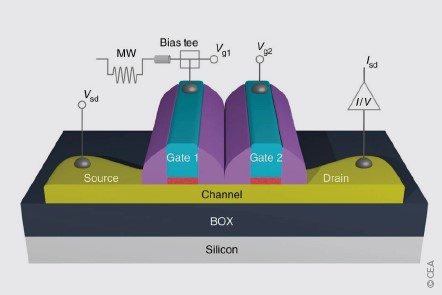
WORLD’S FIRST QUBIT DEVICE FABRICATED IN STANDARD CMOS PROCESS Simplified 3D schematic of a silicon-on-insulator nanowire field-effect transistor with two gates |
- The ability to isolate single electrons within a structure fabricated using CMOS technology. This provides enhanced control over the qubit. As CEA-Leti researcher Maud Vinet put it in a recent interview, the structure is, in essence, "a transistor with huge access resistance. [In that configuration], it’s going to be very easy to [create] a potential well between your two resistances, a quantum dot. And then in this potential well, you can actually trap an electron and come and manipulate its spin with a magnetic field. And this is the story of silicon-spin qubits." To fabricate the quantum dots, CEA-Leti leveraged its FD-SOI platform because it offers several advantages. First, it allows application of capabilities from CEA-Leti’s FD-SOI cryo-CMOS efforts, which have developed CMOS technologies that can operate at cryogenic temperatures. Also, in the development phase, it enables the use of a "back-gate" below the devices to provide in-situ control of the potential wells, which confine the qubits. And additionally, in the context of fabricating a full-stack quantum processor unit with integrated lowtemperature control electronics, FD-SOI appears to be a technology of choice — use of the same technological platforms for qubits and control electronics simplifies co-integration.
- High integration density, which facilitates scalability to larger arrays of qubits. The semiconductor industry has the unique capability to easily and economically fabricate billions of identical micro-structures, such as transistors. Early work done at Quantum Silicon Grenoble has demonstrated the ability to fabricate multi-layer structures that place CMOS quantum dots in close proximity to single-electron transistors (SETsS) with typical spacings of 100nm. This would allow up to 106 qubits to be built in a 100-micron-square (0.1mm) area, with the opportunity for parallel operations — important considerations for a large-scale quantum computing architecture.
Top page