GRENOBLE, France and DELFT, Netherlands – March 1, 2018 – Leti, a research institute of CEA Tech, and Mapper Lithography, the leading provider of maskless lithography equipment for the semiconductor and nanofabrication industries, today announced a low-cost cyber-security breakthrough that encrypts individual chips with a code.
The non-falsifiable code is generated by using a unique chip design that leverages direct multi-beam writing in a process that fits in a conventional CMOS flow with an extra level of lithography and without photomasks. Throughput on Mapper'sFLX-1200 tool installed at Leti is compatible with optical systems.
The markets for these chips include data security, traceability and combatting imports of counterfeit chips.
Leti, a specialist in electron-beam lithography, and Mapper, a Dutch company, presented a paper on the breakthrough, "Process development of a maskless N40 via level for security application with multi-beam lithography", today at SPIE Advanced Lithography 2018 in San Jose, Calif. The paper demonstrates a via patterning integration that is compliant with standard CMOS 40nm process flow.
"Standard optical exposure tools – optical scanners using masks – repeat the identical design on the entire silicon wafer, and cannot fabricate individualized chips," said Leti's Isabelle Servin, the lead author of the paper. "Leti applied its deep multi-beam lithography knowhow and Mapper's unique maskless fabrication tools to achieve this differentiating, cyber-security chip."
The maskless lithography system, based on massively parallel electron-beam writing capability developed by Mapper, is designed for high-volume specialty chips and low-volume advanced logic.
Leti and Mapper are demonstrating the breakthrough for their customers at Leti's facility in Grenoble.
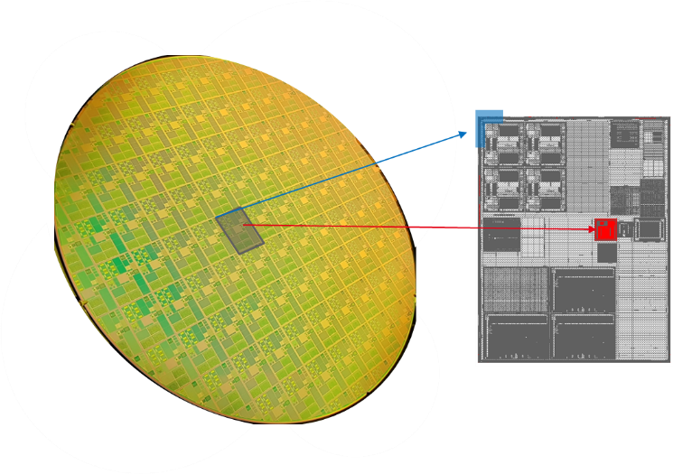
300mm Si wafer exposed on
FLX-1200 multi-beam tool at 5kV on
N40 BEOL stack